SemiNex Opens New Office in Asia to Support Increasing Business in High Power Lasers

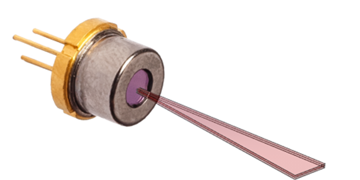
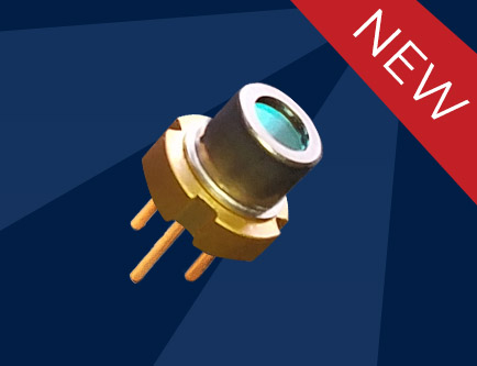
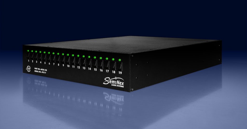
SemiNex Corporation unveils a new sales and application engineering office in Liaoyang, China to support customers with product selection, system integration, pricing and supply across the entirety of the Asian continent. SemiNex now directly supports new business in Asia for high power laser diodes spanning various industries including consumer devices, professional medical, industrial, military and telecommunications markets. Specifically, the fast-emerging LiDAR applications, including those used in autonomous vehicles, will now benefit from this direct support and the introduction of the new SemiNex Multi-Junction Laser with 300% the power of prior best-in-class lasers. The new multi-junction laser diode produces 80 watts at 1550nm with a 95um aperture width yielding more than 3X the power of current single junction laser diodes at this wavelength.

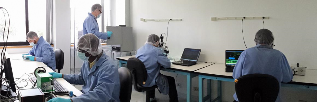
The Asia office will better support new applications and existing business in China, Korea, Japan, and across Asia. This allows SemiNex to showcase these products directly with the Asian consumer, whereas before, it was only possible to do so remotely, especially with limited travel due to COVID-19 restrictions. An increase in sales, customer satisfaction, and further expansion are already being experienced due to the opening of this new office. SemiNex recently presented its products at the CIOE trade show in Shenzen, China, which in normal years attracts over 89,000 professionals. During the show SemiNex supported dozens of applications and a myriad of customers with in-person meetings.

With the inauguration of this new workspace, SemiNex better responds to customer questions, such as product pricing, specifications, product selection assistance and supply inquires. This comes in a year of pandemic challenges, uncertainty and ever changing variables. Despite these circumstances, SemiNex continues conducting successful business throughout the Far East with increasing sales and support of its laser diodes.

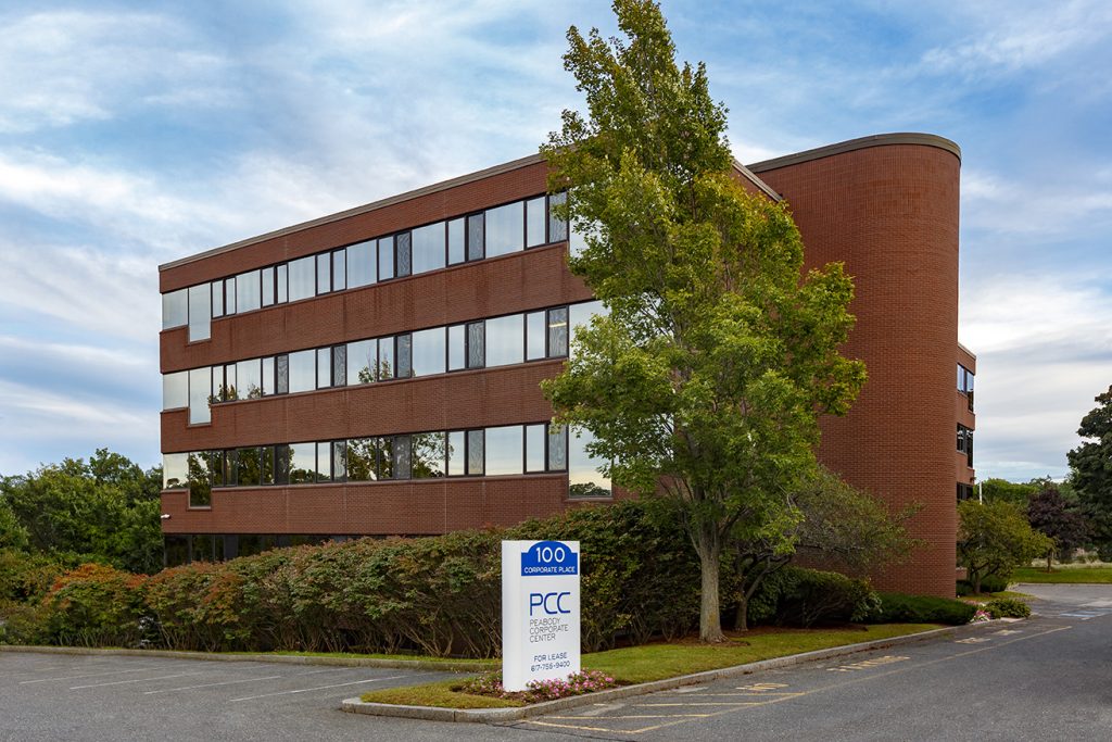
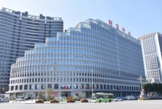
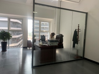
The building, in which the new office is located, is a state of the art structure which recently finished construction. Its central location in Liaoyang allows for easy customer access and convenience, making it effortless to directly schedule in-person meetings, remote calls and web conferences during convenient Asia daily work times. Visitors to the new office will find it contains all the modern amenities one would expect in our present age, providing guests with a comfortable and pleasant experience during their visit. It will serve as a central hub for SemiNex China in the years to come.   

Applications Engineer Hanyu Yang is managing the new Chinese location. Her background includes a master’s degree in engineering from Northeastern University, USA and prior experience at leading medical device companies such as Becton Dickinson Medical. Ms. Yang’s cultural background, international experience and extensive language skills provide our Asian customers with exceptional service.

Ed McIntyre, Vice President of Sales, works closely with Ms. Yang and noted, “I’m very excited about having Hanyu in China to support our customers in real time to bridge the communications gap with direct and timely customer support. That can be very challenging when working on a new engineering project.”

The new office in the Far East has regular business hours from 9am to 5pm China Standard Time (UTC+8) and can be reached at +86 15641953339 / +86 (0419) 5850799,  WeChat 15641953339 or email at hyang@seminex.com.

SemiNex Multi-Junction Lasers Enable Inexpensive, Efficient, Long-Range LiDAR Applications

SemiNex Corporation announces the introduction of a patent-pending, multi-junction, semiconductor laser diode at eye-safe wavelengths between 1310nm and 1550nm with more than 20 times the photons/second and more than 3X the range compared to 905nm LiDAR systems which will enable mass-market auto-driving cars to finally become a reality. The multi-junction laser diode is a drop-in replacement for most compact laser drivers used for existing 9XXnm diode systems. The new SemiNex multi-junction laser diode makes use of 3 monolithic solid-state laser junctions that produce 80 watts at 1550nm with 95µm aperture width and yield more than 3X the power of current laser diodes at this wavelength. Product samples are available immediately and the multi-junction is ready for immediate high volume production.

Typical time-of-flight LiDAR systems using multi-junction 905nm lasers are limited to a range of 100 meters due to eye-safety acceptable emission limits (AEL) of International Electrotechnical Commission (IEC) regulations, thus limiting their use to niche applications such as private security systems, warehouse automation, and limited-use public driving functionality. The new SemiNex multi-junction laser enables high-power, longer-range, lower cost, eye-safe LiDAR solutions for autonomous trains, planes and automobiles.

“SemiNex invested 3 years in research & development to create a long-range and cost-effective solution to overcome the short-range limitations of existing technologies. We see this as a major game changer and believe it will revolutionize the way major LiDAR companies approach this challenge,” said David Bean, CEO of SemiNex Corporation.

The new SemiNex multi-junction laser diode enables eye-safe, autonomous LiDAR systems to reach greater than 250 meters without compromise. Present solutions limit visibility to 100 meters, requiring a vehicles speed to be at 25 mph or less. For the past ten years LiDAR manufacturers have taken two laser approaches for time-of-flight LiDAR systems: 905nm laser diodes or 1550nm fiber lasers. The 905nm laser diodes suffer from limited range due to eye-safety regulations and the 1550nm fiber lasers are impractical for mass market deployment because of their size and cost. Until now, there was no solution that offered the low-cost, small size, and efficiency of 905nm laser diodes with the eye-safety and extended range of 1550nm fiber lasers.

Neither of these past approaches meet the automotive industry goals to enable LIDAR commercialization. The lack of efficient and inexpensive 200 meter eye-safe LiDAR has held back the industry from commercializing autonomous vehicles and seeing any meaningful mass-market deployment at speeds greater than 25 mph. “The SemiNex multi-junction laser diode changes everything,” states Ed McIntyre, SemiNex Director of Sales & Marketing. “Now there is a low-cost, long-range, eye-safe alternative to 9XXnm diodes and 1550nm fiber lasers.”

Today, the LiDAR market for automotive and industrial applications is expected to be $981 million and limited to short range applications. However, with improvements in technology and broader acceptance, the market is expected to grow to $2.8 billion by 2025. A major challenge with the existing LiDAR technology for autonomous vehicles has been to find a cost-effective semi-conductor laser diode that can provide high peak power at eye-safe wavelengths for long range applications. Operating at 1550nm, the SemiNex triple junction device provides 3X the peak power of a single emitter thus improving the resolution and penetration effectiveness in bad weather while remaining eye-safe. It can be operated at pulse widths between 2ns and 100ns at 200kHz to 400kHz pulse repetition rate. SemiNex offers multi-junction devices between 1310nm and 1550nm at various aperture widths and cavity lengths to meet specific customer requirements.

“The SemiNex multi-junction laser diodes will allow vehicles to autonomously navigate at higher speeds that can’t be achieved with the existing technology; this could finally enable driverless cars to be a reality within the next 5 years,” suggests McIntyre.

The multi-junction device is available in double and triple junction configurations in various packaging and submount configurations. Samples in either TO-9 or bare die configuration at 1550nm are available for immediate delivery.

For more information visit www.seminex.com or visit us at CIOE trade show in Shenzhen, China, September 11th– 13th Booth #2D80. To schedule a meeting with Hanyu Yang, our Applications Engineer, click here.

Seminex Aims to Revolutionize Home Skincare with Lasers

NIRA

SemiNex Corporation is pleased to announce its collaboration with Dermal Photonics Corporation, maker of NIRA Skin, to bring professional dermatology laser technology to the home market at an affordable price. The NIRA Skincare Laser is the first of its kind, delivering dramatic and lasting improvements by stimulating natural collagen production to renew skin without causing pain or redness. The NIRA Skincare Laser holds 12 patents and is FDA-cleared with proven safety and efficacy based on clinical studies that were reviewed and cleared by the US government.

SemiNex is a major supplier for laser diodes for professional dermatology systems with over 15 years of experience supply to laser components for non-ablative fractional and non-fractional laser system.  To enable these types of non-ablative laser treatments for in-home use, SemiNex developed a patented low-cost packaging named the Laser Engine. The high-volume, low-cost Laser Engine enables Dermal Photonics to use the same laser diodes as a professional system in a cost-effective solution for the home market. SemiNex developed production capability to build over 100,000 units annually with plans to grow further as needed.  

SemiNex is proud to partner with Dermal Photonics who designed, assembles and manufactures their products in the USA. The skin-care market makes up about $100 billion with $40 billion focused on anti-aging skincare.

SemiNex is delivering an eye-safe 1450nm laser engine to Dermal Photonics for their NIRA Skincare Laser. The light being emitted from the SemiNex laser within the NIRA Skincare Laser is absorbed deep in the dermal cells and releases proteins which signal the body to rejuvenate and renew the skin. SemiNex provides Dermal Photonics best-in-class laser technology that provides real and dramatic results while avoiding all the traditional issues with lasers such as high cost, pain, redness (erythema), and difficulty of use.

Laser Engine

Customers from all over the world are noticing a difference. “My face has not looked this young or this good in more than a decade. This product was painless and delivered amazing results,” said one NIRA Skin customer in their product review.

In December 2019, NIRA was featured on Ideal World, a UK home shopping network, for the first time and it was a major success. They sold out of their allotment of NIRA Skincare Lasers within the first show and had to rush 3 additional shipments overseas to the Ideal World England warehouse to keep up with demand. The product was so successful that Ideal World has brought back NIRA for two additional weeks and is scheduled to hold a “Pick of the Day” special promotion soon. 

“With the present COVID-19 situation, we are finding people who would normally go to their professional dermatologist or medical spas for treatments, can now treat themselves in the comfort of their own home using the NIRA Skincare Laser,” commented David Bean, Founder/Inventor of Dermal Photonics.

David Bean

If you have any requests or inquiries, we are here to assist and support. Please contact us by e-mail at sales@seminex.com or at info@seminex.com.

About NIRA Skin:

NIRA Skin is committed to providing the newest generation skincare solutions to help improve the health and beauty of your skin. We believe everyone should have access to professional-level skincare at home and at an affordable price. NIRA Skin brings you the same technology used by professionals into the home, with an easy-to-use program that is enjoyable to use and guarantees results.

Learn more at www.NIRAskin.com.

For additional information please contact NIRA Skin at info@niraskin.com.

COVID-19 – How we are managing in these uncertain times

First and foremost, we hope you and your family are well. During this period of uncertainty, we feel a major responsibility in helping slow the spread of COVID-19 in the US. Our office is taking every precaution to ensure the health and safety of our clients, colleagues, and staff while remaining fully functional during this worldwide crisis.

Our sales teams and most office staff are fully equipped to work remotely and meet the needs of our customers. Meanwhile, our operation team is ensuring business continuity by working in small shifts and strict procedures to keep safe and effective operations.

We are focusing our attention on meeting our delivery commitments to all our customers and most importantly we support medical projects like the Veralase laser vaccine adjuvant development that will increase the efficacy of vaccinations up to 10X when a COVID-19 vaccine is discovered. As a key supplier of critical components into defense and medical industries, SemiNex is designated as an “essential” business and we continue to work through this crisis and to support important medical development and other critical industries.

Specifically, at SemiNex we are applying the follow procedures to ensure safety:

  • -No in-person visitors; we encourage phone and web-conferences
  • -General hygiene and safety precautions
  • -Important actions for safety at the workplace
  • -Sanitizing the workplace and maintaining hygiene
  • -Safety of shared surfaces (meeting rooms, work desks, bathrooms etc.)
  • -Screening of visitors
  • -Travel on hold
  • -Reducing large gatherings and meetings
  • -Elbow bump instead of handshakes

We thank you for your understanding and cooperation through this extraordinary period of time. We will keep you informed of any significant changes.

If you have any requests or inquiries, we are here to assist and support. Please contact us by e-mail at sales@seminex.com or at info@seminex.com.

LMU MUNICH and MPQ Reveal Direct Diode-Pumped KLM Cr:ZnSe Oscillator

Research by a joint team of scientists from the Max Planck Institute of Quantum Optics and the Ludwig Maximilian University of Munich has led to the first directly diode-pumped Kerr-lens mode-locked Cr2+-doped II-VI oscillator capable of providing average output powers over 500 mW using a SemiNex diode as the diode source. This development will reduce the cost dramatically by more than 5X over the existing common fiber laser technologies available on the market today.

“With this new class of cost-effective and table-top driver for mid-infrared generation, we have taken a crucial step in providing a more accessible alternative to synchrotron-like infrared radiation,” emphasized Nathalie Nagl, Ph.D. student at the LMU Munich.

Cost-efficient MIR sources are requisite to meeting the growing demand in a spectroscopy market estimated to be worth $1.27 Billion by 2022¹. Known as the molecular “fingerprint region,” the mid-infrared can be used to accurately identify samples for pharmaceutical, defense, food safety and manufacturing processes.

The performance of the team’s solution rivals larger, more costly fiber-pumped oscillators by yielding 2.5-times the peak power compared to previous Cr:ZnSe oscillators at 45 fs pulse durations and delivers outstanding low-noise performance.

Other efforts to directly pump Cr:ZnS/ZnSe crystals using diodes in the 1.5-1.6 um regime have been hampered by heat-related issues. SemiNex InP diodes are designed to provide the best thermal performance and highest brightness at these wavelengths in the market today.

“SemiNex is constantly looking to participate with companies and universities to develop innovative technologies that will open new markets for us to participate in. This new approach will impact the availability of lower cost/higher performance portable spectroscopic devices in the mid-IR range,” commented Ed McIntyre, head of Business Development at SemiNex Corporation.

The results of the project were presented at the CLEO conference during this year’s Laser World of Photonics in Munich, and have recently been published in the journal Optics Express². For inquiries about the research team, please contact Nathalie Nagl at Nathalie.Nagl@physik.uni-muenchen.de.

Visit SemiNex at Booth #163 at Photonics West Moscone Center, San Francisco, CA, or schedule a meeting with Hanyu by clicking here.

¹ https://www.photonics.com/Articles/Life_Sciences_Demand_Spurs_Spectroscopy_Market/a61584

² https://www.osapublishing.org/oe/abstract.cfm?uri=oe-27-17-24445

Hanyu Yang Named New Application Engineer

Hanyu Yang

SemiNex Corporation is pleased to announce the hire of Hanyu Yang for the role of Application Engineer. Ms. Yang will be responsible for providing sales and technical support to customers and recommending new products for development to the engineering team based on market demand.

Before coming to SemiNex, Ms. Yang assisted in preparing design validation tests and preclinical reports for Becton Dickinson Medical. She was also instrumental in scripting and creating product training videos for their line of insulin pumps.

“I was attracted to SemiNex by the company’s mission to produce high-power diodes in the eye-safe wavelength range especially in the LiDAR market,” Ms. Yang said. “I believe that enabling our customers to consider human factors in their projects is the best multiplier to truly create change.”

A graduate of Northeastern University with a Masters in Engineering Management, Ms. Yang brings to bear her experience writing technical materials in both English and her native Mandarin Chinese.

“We’ve been seeing an uptick of inquiries for infrared applications coming out of the technology sector in China,” said Ed McIntyre, VP of Business Development. “Hanyu’s insight into these markets allows us to more fully communicate with these prospects. She’s already been invaluable in planning our booth for CIOE in Shenzhen this September.”

Visit SemiNex at Booth 3L11 at CIOE Shenzhen, or schedule a meeting with Hanyu by clicking here.

SemiNex Unveils New TO56 Mini at Laser World of Photonics

Sample pieces will be on display at Booth B3-511 June 24 through June 27 at Laser World of Photonics in Munich, Germany.

TO56 Mini

SemiNex Corporation now offers high performance, low-cost TO-56 “Mini” submounts targeted toward pulsed laser applications, such as OTDR, long distance range-finding, and LiDAR. This breakthrough design has the same 5.6mm diameter of the standard SemiNex 1.50 mm laser diode packaged in a TO-56 to enable convenient drop-in replacement with existing TO-56 systems with a body length of only 4.3mm.

“Our customers anticipate market demands of 100k units and beyond. At those volumes cost savings are critical and this product is designed to meet both performance and cost targets,” says Ed McIntyre, VP of Business Development. “With the Mini, we provide best-in-class optical and electrical performance in a standard TO-56 radial form factor while passing on the benefit of reduced costs.”

SemiNex offers industry-leading 5 mrad fast-axis laser collimation lensing as a product option for all laser apertures. Alternatively, SemiNex provides collimation-matching of the fast- and slow-axes for systems designed to make use of this collimation parity to focus the light with bulk optics outside of the TO-56 package. These options are included for the new TO-56 Mini. Aperture widths of 50µm, 95µm, 180µm and 350µm are available with peak powers from 10 to 30 Watts.

“The TO-56 Mini package is half of the height of our standard SemiNex TO-56 package,” says Seth Pappas, lead Product Engineer, “and powerful enough to generate 25W pulsed at 1550nm. For manufacturers of handheld OTDR devices, portable LIDAR systems, and range-finders, this is a winning combination.”

The TO-56 mini is available for immediate delivery at the following eye-safe wavelengths: 1310nm, 1550nm, 1625nm and 1650nm. Other wavelengths can be provided upon request.

SemiNex Launches Laser Engine Production Line

As of March 2019, SemiNex Corporation begins manufacturing their laser engines on a newly implemented assembly line at their headquarters in Peabody, Massachusetts.

Over the past couple years SemiNex engineers have optimized trial production processes to lower cost, improve performance and increase capacity. Now with production in full swing, SemiNex will continue to monitor and improve key performance metrics such as cycle time, on-time delivery, yield, and throughput. These steps will be crucial to successfully transfer the process over to contract manufacturing – a technique that SemiNex typically uses to stay lean.

“The new production line uses custom fixtures to automate critical steps and requires minimal input from a technician,” says Mechanical Engineer and project lead, Matt Hamerstrom. “We’ve reduced assembly time 10 fold from the old design, and we were able to halve the cost while maintaining optimal performance.”

While there has been considerable interest in home laser treatments, few companies have been able to produce laser devices at a price and safety standard appealing to consumers. Every component of SemiNex’s new production line, from the custom fixtures to the software on the final test station, has been engineered to meet these requirements for the consumer beauty market.

“It’s been invaluable to have the insider knowledge and experience SemiNex brings to the production process,” says Kayla Govoni, spokesperson for NIRA, a manufacturer of handheld home skincare laser devices. “We’re expecting 2019 to be the year we really start seeing lasers for aesthetic use inside people’s homes.”

SemiNex Announces 19 Laser Module at Photonics West

SemiNex Corporation is pleased to announce that it will feature a new design at Photonics West, Feb 5 through 7 at Booth # 5286.

SemiNex Corporation is pleased to announce we will be featuring our new 19 laser module at the sold out SPIE Photonics West Conference in San Francisco, California.

“In contrast to the other products in the existing SemiNex MCM family which utilize fiber bundles to achieve high power emission, this module couples our existing InP laser chips with fusion spliced fiber technology and is packaged to maximize efficiency and power requirements,” explains Ed McIntyre, VP of Business Development. “We’re anticipating this product will appeal to hospitals and research institutions; the versatility of wavelength mixing in a single unit provides enormous value.”

Designed to be 2U rack mountable, this high powered unit can produce up to 100W of CW power through the single 600um/0.22NA main output fiber, and allows the consumer to individually control and combine up to 19 lasers at wavelengths from 1250 to 1940nm. Internally mounted TECs are available for each laser diode source allowing for wavelength tuning via temperature. For overall thermal management the device comes with a water cooled chiller plate with inlet and outlet ports for coolant.

Click here to arrange an appointment at the conference with Ed McIntyre, head of Business Development or here to meet with Patrick Dinneen, Lead Applications Engineer.  See you there!

Share our excitement for the show but can’t make it out to San Francisco? You can still participate in our giveaway as seen on Photonics.com – mention “SPIE2019” to receive a unique gift with your next order!

SemiNex Increases Production Space

SemiNex Corporate Headquarters

SemiNex Corporation has acquired an adjoining suite to their current headquarters in Peabody, Massachusetts effectively doubling production area and increasing office space. This move complements several rounds of hiring and paves the way for several product releases anticipated in 2019.

“For more than 10 years, SemiNex has kept costs down for customers by operating with a streamlined fabless business model,” explains David Bean, SemiNex President. “In the coming year, we’re predicting a substantial increase in demand for our wavelengths within the consumer market. Our expansion will enable us to seamlessly accommodate these new high volume orders without impacting our existing customer base.”

The new clean room facilities are designed to meet ISO Class 7 standards and ESD best practices, and are expected to be fully outfitted with upgraded test stations and equipment by January of 2019. The suite also includes office space for SemiNex engineers and process technicians.

“We’ve designed additional automation into our manufacturing processes and expanded our testing capabilities, freeing up lab space for R&D and specialty fabrication projects,” says Product Engineer Seth Pappas.

en_USEnglish